


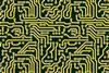
Photolithography is a useful and common tool in technology, and this session will show learners how to create their own circuit boards
This session should take five and a half hours.
Suggested timings
- 10.00 Student registration
- 10.30 Welcome and introductory talk
- 11.00 Hands-on session
- 12.00 Lunch and chance to visit exhibition stands
- 12.45 Lecture (chemistry exam advice)
- 13.30 Hands-on session (teachers go to ICT training session)
- 14.30 Break
- 14.45 Interactive quiz (with prizes)
- 15.30 Finish
Equipment
- Eye protection
- Gloves
- Circuit board
- Tweezers with a small rubber band
- UV light box
- Permanent marker pens
- Photomasks (circuit board patterns on acetate sheets) x 2
- Photoresist developer applicators x 10
- Photoresist stripper applicators x 10
- Beakers
Chemicals
- Iron(III) chloride solution
Health, safety and technical notes
- Read our standard health and safety guidance here.
- Wear eye protection, and gloves, at all times.
- Perform a risk assessment for this activity.
- Be careful not to over-etch. If you leave the board in the solution for too long, the copper that is protected by the photoresist will also etch away.
Procedure
Exposing the photoresist
- Get a piece of circuit board. It has black tape covering one side that protects the underlying photoresist layer from the light. On the side without the black tape, write your initials using a permanent marker pen. Make sure that you write clearly and in bold lettering, as the etching process may remove some of the ink.
- It is very important to hold the board by the edges and not get any fingerprints on the board. Peel off the black tape to reveal the photoresist.
- Place the circuit board over one of the patterns on the photomask, photoresist side down (side without your name).
- When all the circuit boards are ready, the demonstrator will turn on the light box for 80 seconds.
Developing the photoresist
- After the UV exposure has ended and the light box has been turned off, retrieve your circuit board. You should be able to see a faint pattern in the photoresist on your circuit board. The exposed photoresist will have a slightly more yellow colour than the unexposed region, which appears metallic green.
- Check the developer applicator sponge. If it looks dirty, clean with a damp paper towel.
- Gently dab on the developer (do not rub) using the applicator sponge. Cover the entire photoresist surface, including the edges. The developer will remove the exposed photoresist.
- As soon as you can see the shiny copper, rinse off the developed photoresist with water to reveal the copper underneath.
- Inspect the pattern. If there are bits of dirt, rinse them away with water.
Etching the copper
- Wrap a small rubber band around the tweezers so that they stay closed
- Use the tweezers to pick up the developed circuit board, being careful not to touch the photoresist pattern. Set a timer for 10 minutes.
- Dip the circuit board into the iron(III) chloride solution to etch the board. Make sure that the entire board is covered. Gently swirl the solution occasionally.
- After 10 minutes start checking the board to see if etching is complete. Remove the circuit board and dip it into clean water in a plastic tray. Look to see if the copper that is not protected by the photoresist is completely etched away, revealing the plastic underneath. If the copper is not completely etched, place the board back into the solution.
- When etching is complete, wash the circuit board in clean running water.
Stripping the photoresist
- Dab on the photoresist stripper to dissolve the photoresist that is covering the copper pattern.
- Rinse with running water.
- The copper pattern should appear shiny and metallic.
Questions
- What are some of the sources of error in the photolithographic process?
- What are the limitations that determine the minimum sized feature that can be produced by photolithography?
- Other than increased speed, what are the advantages of making chips smaller?
Answers
- Misalignment of mask to substrate, over/under exposure, over/under etching etc. Each step is very sensitive and must be done carefully.
- The photoresist is patterned by UV light. Features cannot be smaller than the wavelength of light (365 nm) unless some optical ‘tricks’ are played. For smaller features, electron beams are used to pattern photoresists.
- Increased portability, parallel processing (lower production costs), lower material costs, greater durability
Downloads
Photolithography resource
Experiment | PDF, Size 0.7 mb


No comments yet