Additions and corrections
Analysis of the operation of thin nanowire photoelectrodes for solar energy conversion
Justin M. Foley, Michelle J. Price, Jeremy I. Feldblyum and Stephen Maldonado
Energy Environ. Sci., 2012, 5, 5203–5220 (DOI: 10.1039/C1EE02518J). Amendment published 23rd August 2012.
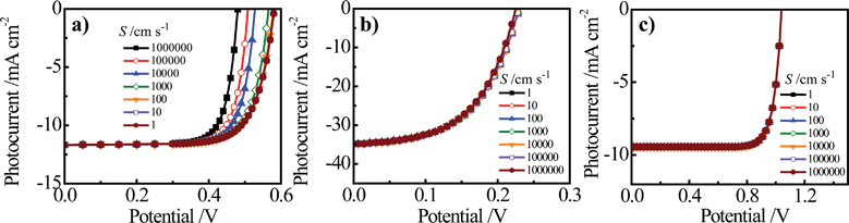
The image of Fig. 8 on page 5215 is wrong as the labels inside Fig. 8a have been inverted. The correct image is given below
| ||
| Fig. 8 Simulated current–voltage photoresponses under AM 1.5 (direct + circumsolar) illumination of (a) a 100 µm thick planar n-Si photoelectrode, (b) an n-Si nanowire photoelectrode with a radius of 50 nm and a height of 100 µm, and (c) an n-GaP nanowire photoelectrodes with a radius of 50 nm and a height of 100 µm across a range of surface recombination velocity, S, values. The full sets of optoelectronic values used in these simulations are collected in Tables S8 and S9. | ||
The Royal Society of Chemistry apologises for these errors and any consequent inconvenience to authors and readers.
Back to article